Currently, superconductive circuits are considered one of the most promising candidates for storing information in future quantum computers. These superconductive circuits may have the capacity for extremely high processing ability to solve complex problems that are too time consuming for current computer systems.
A common method for constructing superconducting quantum circuits is coupling them with coplanar waveguide (CPW) resonators. However, using a completely flat geometry creates limitations in building complex devices, as we cannot pass wires over each other in two dimensions. In addition, the symmetric coplanar waveguide geometry which used ideally in quantum circuits keeps ground surfaces at the same voltage on both sides of the centerline. Because asymmetry and discontinuity in the microwave circuit can cause excitation of parasitic modes. These modes can couple to circuit elements such as qubits and be a source of loss and decoherence. To suppress these modes and enable more complex wire routing, we need three-dimensional wiring such as superconducting air bridges.
Researchers at the Quantum Computing (IQC) have introduced a new single-step process for constructing small bridges on superconductive circuit microchips, which are essential for future quantum computers based on superconductors.
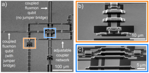
These small bridge structures, known as air bridges and shown in figure 1, are used to create complex designs. They enable passage through various parts of the circuit and reduce data loss in existing superconductive circuits on microchips.

Figure 1. A scanning electron microscope image of the air bridges used in superconducting quantum circuits.
Noah Janzen, a PhD student in the Department of Physics and Astronomy at IQC and the lead author of this article, said, “Our new method creates strong air bridges using just one lithography step. With our single-step process, the time, cost, and materials required to create these structures are significantly reduced and optimized compared to previous well-known air bridge fabrication processes.”
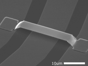
Air bridges are very small, for example, the width of the bridge shown in figure 2 is 6 micrometers, over 10 times smaller than a hair strand. Typically, the length of these bridges will be between 20 to 100 micrometers (at their largest, the size of a single hair). These bridges improve the quality of microchip devices by reducing quantum decoherence effects.

Figure 2. A scanning electron microscope image of a 36-micrometer long aluminum air bridge fabricated using a one-step electron beam lithography process.
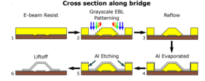
To create air bridges, the research team placed a polymer (photoresist) on top of the microchip and then used a focused beam of electrons to create a three-dimensional pattern for the bridge using a process called electron beam lithography. Then, a thin layer of aluminum was deposited on the top of the bridge template. Finally, the polymer template was removed, leaving only the aluminum bridge suspended in the air. The schematic design of the construction process is shown in the figure 3.
Air bridges are an important element for improving the quality of superconducting circuits and also open up the design space for these circuits from 2- dimensions to 3-dimensions. Combined with the newly reported simple method for creating air bridges, this provides researchers with a process to create more complex microchips and devices.

Figure 3. Schematic diagram of the fabrication steps of the air bridge.
References:
[1] Janzen, Noah, Michal Kononenko, Shaun Ren, and Adrian Lupascu. “Aluminum air bridges for superconducting quantum devices realized using a single-step electron-beam lithography process.” Applied Physics Letters 121, no. 9 (2022): 094001.
[2] https://uwaterloo.ca/science/news


